In the precision chain of microelectronics manufacturing, wire bonding technology acts as a "microscopic bridge," establishing a crucial connection between chips and external circuits. As the most common and important application of ultrasonic welding in this field, this technology, with its unique advantages, supports the large-scale development of the semiconductor packaging industry and has become an invisible cornerstone for the reliable operation of electronic devices.
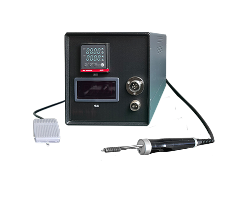
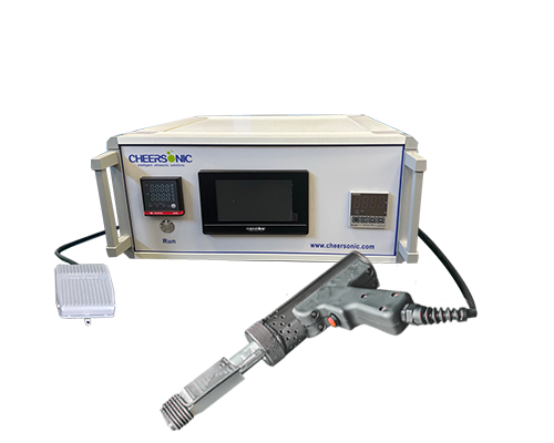
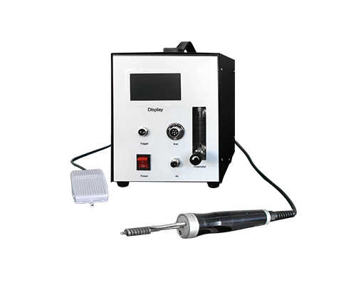
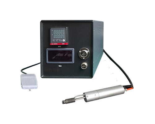
The core principle of wire bonding is to use ultrasonic energy to achieve atomic-level bonding between metals. During the packaging process, the equipment removes the oxide layer on the surface of the metal wires and chip pads through high-frequency vibration. Under the synergistic effect of pressure, the two metals form a strong connection. The entire process does not require high-temperature melting of materials, and the heat-affected zone can be controlled below the millimeter level, perfectly avoiding the risk of chip thermal damage that may be caused by traditional processes. This characteristic makes it an ideal choice for packaging precision microelectronic devices, with wide applications ranging from consumer electronics to aerospace equipment.
The maturity and reliability of the technology have made wire bonding dominant. Currently, more than 60% of semiconductor packaging relies on this technology, making it almost irreplaceable in traditional packaging forms such as QFP and BGA. Its bonding strength can be optimized through precise control of ultrasonic power, pressure, and other parameters. Combined with tensile testing and failure analysis, it ensures the stability of the solder joints under harsh environments such as vibration and temperature differences. This is a key reason why this technology is prioritized in high-end fields such as medical equipment and satellite payloads.
Cost-effectiveness and material compatibility further solidify its core position. Compared to technologies like flip-chip bonding, wire bonding equipment requires less investment and is compatible with various metal wires such as gold, copper, and silver. The use of copper and silver wires not only reduces the consumption of precious metals but also meets the requirements for high conductivity. Improved materials such as palladium-plated copper wire solve the oxidation problem, balancing economy and performance.
As microelectronics continues to evolve towards miniaturization and high density, wire bonding technology is constantly being upgraded. The addition of features such as automatic resonant frequency tracking and real-time energy monitoring controls amplitude fluctuations within ±0.5μm, significantly improving the welding yield of precision components such as 5G communication modules.