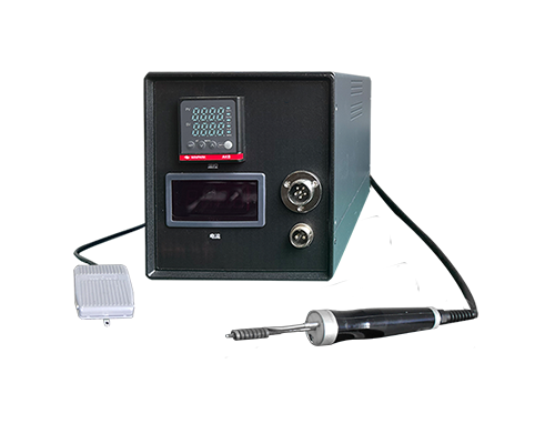
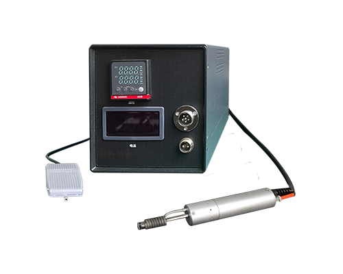
In the semiconductor packaging field, ultrasonic copper wire bonding, a core connection technology, acts like a precise "microscopic bridge builder," establishing a reliable electrical path between the chip and external circuitry. Its performance directly determines the stability and lifespan of electronic devices. This technology, which integrates ultrasonic physics and materials science, is continuously evolving with the trend of miniaturization in the microelectronics industry.
The core principle of ultrasonic copper wire bonding is the synergistic effect of pressure, ultrasonic energy, and temperature. During bonding, the capillary of the wire bonder precisely grips a high-purity copper wire, just a dozen microns in diameter, and uses an arc to melt the end into a uniform gold ball. Then, under pressure, the gold ball is pressed firmly against the chip pad. Simultaneously, high-frequency ultrasonic energy is transmitted to the contact surface by a cleaver, causing the atoms on the metal surface to vibrate violently, breaking down oxide layers and contaminants. Ultimately, atomic diffusion forms a strong metallurgical bond. This solid-phase bonding method eliminates the need for high-temperature welding, thus avoiding thermal stress damage to the chip, a significant advantage over traditional soldering.

Process precision is crucial to the success of this technology. Before bonding, plasma cleaning is required to ensure the pads are free of impurities. The wire bonder's positioning accuracy and ultrasonic power output are also calibrated. During the bonding process, each step—gold ball formation at the first solder joint, wire arc tension control, and positioning and pressure bonding at the second solder joint—requires coordinated parameter adjustments. Experiments have shown that with a bonding time of 1100ms, an amplitude of 40%, and a pressure of 0.3MPa, the joint tensile strength can reach 554.8N, with a resistance as low as 0.275mΩ. Post-bonding, microscopic inspection is required to detect defects such as cold solder joints and broken wires to ensure connection quality.
This technology's widespread adoption stems from its significant advantages. Copper wire's high electrical and thermal conductivity allows for rapid heat transfer from the chip, and its cost is significantly lower than traditional gold wire. Its micron-level operation meets the high-density packaging requirements of miniature devices such as smartphones and IoT sensors. However, the technology still faces challenges: copper easily oxidizes, requiring nitrogen protection or surface coating. Excessive growth of intermetallic compounds can lead to brittle solder joints, which requires parameter optimization to prevent. As electronic devices advance toward higher integration and longer lifespans, ultrasonic copper wire bonding technology is reaching new heights. Process optimization and equipment upgrades are continuously expanding the parameter window, and new surface treatment technologies are enhancing oxidation resistance. This microscopic "needle-threading" technology has become a core cornerstone supporting the high-quality development of the microelectronics industry, continuously providing stable and reliable connection solutions for various smart devices.