In fields such as microelectronics packaging and aerospace, the combination of glass, due to its excellent optical properties and stability, and metal, due to its excellent electrical and thermal conductivity, is crucial for achieving the functionality of high-end devices.
However, due to the significant differences in the physical and chemical properties of glass and metal, bonding faces three major challenges: poor wettability, mismatched thermal expansion coefficients, and difficult interfacial reactions. Traditional active brazing is costly, complex, and exacerbates thermal stress, while adhesive bonding poses issues such as aging and insufficient airtightness.
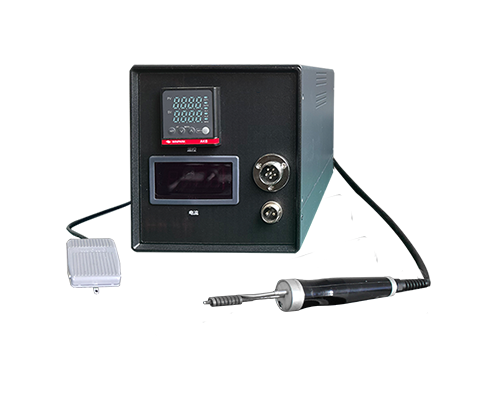
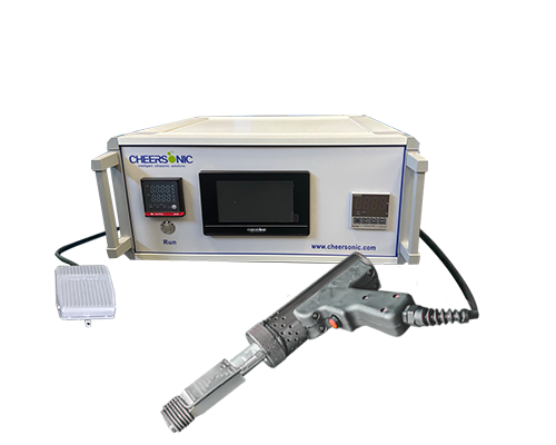
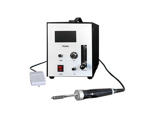
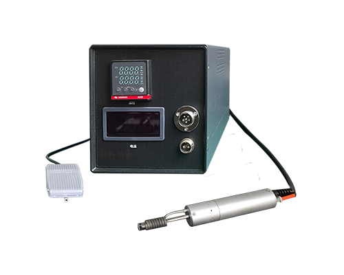
Ultrasonic-assisted brazing technology offers a new approach to addressing these issues. Its core approach involves introducing 60kHz high-frequency mechanical vibrations into the molten brazing material, generating cavitation and acoustic streaming effects. The cavitation effect instantly generates high temperature and pressure, breaking the chemical bonds between the metal oxide film and the glass surface and promoting interfacial reactions. The acoustic streaming effect stirs the brazing material, removes impurities, and enhances mass transfer.

This technology achieves interfacial bonding through a combination of mechanical anchoring, chemical bonding, and acoustic oxidation reactions. Mechanical anchoring leverages the surface roughness of the glass to enhance joint strength. Chemical bonding is key to high-strength connections, such as the formation of specific chemical bonds between tin solder and glass. Sono-oxidation reactions can generate a nano-oxide layer at low temperatures, bridging the gap between the solder and the substrate.
Process parameters significantly influence ultrasonic brazing quality. Too low ultrasonic power results in low bond strength, while too high may damage the substrate. Too short ultrasonic time results in incomplete reaction, while too long can lead to performance degradation. The temperature must be appropriate to ensure solder flow while avoiding excessive thermal stress. Low-melting-point Sn-based solders with active elements are the mainstream, and the active element content must be optimized.
This technology holds broad application prospects in optoelectronics, new energy, aerospace, and other fields. Future research is needed in process automation, solder design, reliability assessment, and application expansion to further enhance its role in high-end manufacturing.