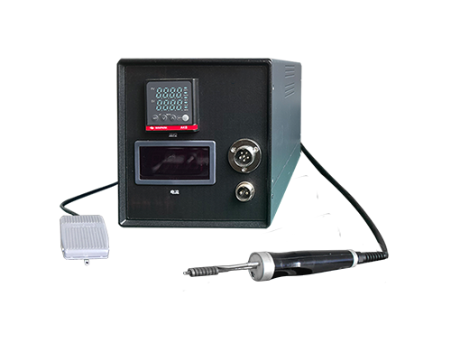
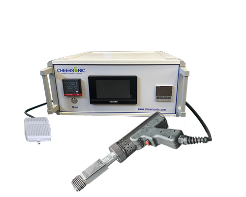
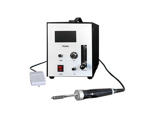
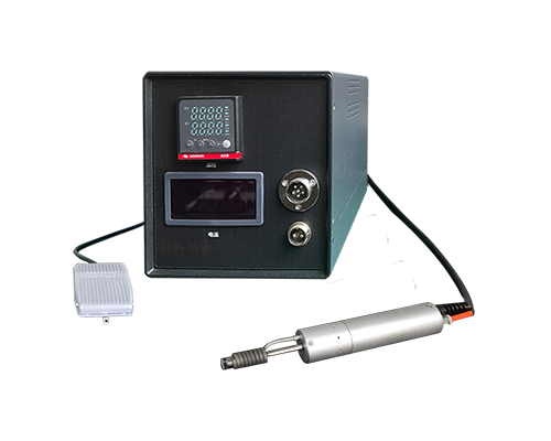
In ultrasonic microelectronics, gold and silver wire bonding are key processes for achieving electrical connections between chips and external circuits, decisively impacting the performance and reliability of electronic products.
Gold wire bonding has become a mainstream choice for semiconductor packaging due to its numerous advantages. Gold's excellent ductility allows it to adapt to complex shapes during the bonding process, ensuring a tight bond. Its excellent conductivity effectively reduces resistance during signal transmission, ensuring fast and stable signal transmission, which is crucial for microelectronic devices that demand extremely high signal processing speeds. Furthermore, gold wire bonding provides sufficient bond strength, ensuring a stable connection and reducing the risk of connection failure caused by vibration, temperature fluctuations, and other factors during product use. Furthermore, it easily forms a well-defined wire loop shape, helping to optimize internal chip wiring layout and improve space utilization. Gold wire bonding is typically achieved using thermocompression ultrasonic bonding, a method that cleverly combines heat and ultrasonic energy. Hot pressing initially bonds the gold wire to the pad under a certain temperature and pressure, while ultrasonic energy further promotes interdiffusion and fusion between metal atoms, significantly improving bond quality. Compared to simple hot pressing, hot pressing and ultrasonic bonding reduces processing temperatures, avoiding potential damage to the chip caused by high temperatures. It also enhances bond strength, effectively ensuring device reliability.

Silver wire bonding also demonstrates unique value in specific scenarios. From a cost perspective, silver is cheaper than gold, significantly reducing material costs in large-scale production. In applications requiring high light reflectivity, such as LED devices, silver wire's high reflectivity can improve luminous efficiency and optimize product performance. Silver wire becomes an ideal bonding material when the chip pad is sensitive and copper cannot be used, as it is easily damaged by copper's high bonding strength. However, silver wire bonding also faces challenges. For example, silver is chemically reactive and can oxidize under certain conditions, affecting the long-term stability of the bond. This necessitates special protective measures during the bonding process, such as performing the bonding operation in a specific protective atmosphere to reduce the risk of oxidation.
During the bonding process, many factors affect bond quality. Ultrasonic power significantly impacts bonding. Excessive power causes violent movement of metal atoms, creating large voids in the bonding area. This reduces the bond area, weakens the weld strength, and can even cause plastic deformation of the wire. Insufficient power fails to effectively remove impurities and oxides in the bonding area, significantly reducing bond strength and, in severe cases, preventing the bonding operation from being completed. The duration of ultrasonic exposure is also crucial. Too short an exposure fails to completely remove the adhesive layer and oxide film on the gold wire and the surface of the chip being bonded, hindering the formation of a strong metallurgical bond between atoms and leading to debonding. Too long an exposure can reduce the mechanical strength of the solder joint and, in extreme cases, damage it. Bonding pressure is also crucial. Insufficient pressure prevents a secure connection between the gold wire and the pad and may cause the wire to adhere to the blade tip. Excessive pressure can lead to excessive deformation or even breakage of the gold wire, potentially damaging the metal layer on the chip surface.
Gold and silver wire bonding each have their own advantages in ultrasonic microelectronics. With the continuous advancement of microelectronics technology, the requirements for bonding processes are also increasing. In the future, researchers will continue to optimize bonding process parameters and develop new bonding materials and technologies to meet the needs of microelectronic devices towards smaller size, higher performance, and lower power consumption, and to promote the continuous advancement of the entire field of ultrasonic microelectronics.