In the microscopic world of semiconductor packaging, the connection between chip electrodes and the substrate is a core element determining device performance. This connection must not only achieve stable electrical conduction but also bear multiple functions such as signal transmission, heat dissipation, and physical support. Its technological evolution has always kept pace with chip miniaturization and high performance.
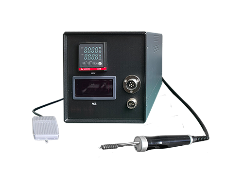
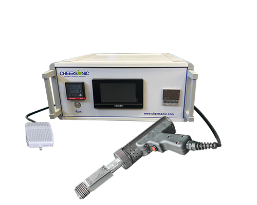
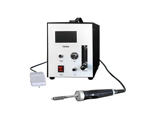
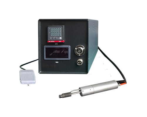
Wire bonding technology is a "perennial" in the field of interconnection, occupying an important position in semiconductor manufacturing processes due to its mature and reliable characteristics. This technology interconnects the electrode pads at the chip edge with the substrate using metal wires. Gold wires are commonly used in high-reliability scenarios, aluminum wires are suitable for low-cost requirements, while copper wires are emerging as a choice due to their excellent conductivity. During the bonding process, the energy action of thermo-pressure, ultrasonic waves, or a combination of both can form a strong bond between the wire and the pad. Ball bonding and wedge bonding methods are suitable for different wire materials and precision requirements, respectively. However, the presence of wires increases the package size, and the longer transmission path may introduce parasitic parameters, making it difficult to meet the requirements of high-density interconnection.
The emergence of flip-chip bonding technology has broken through the density bottleneck. The core of this technology involves placing the chip face down and directly connecting it to the substrate via an array of bumps, eliminating the need for lead wires and shortening the signal transmission path by more than 50%. The process flow includes three steps: bump fabrication, chip assembly, and underfill. Reflow soldering melts the bumps to form connections, significantly improving I/O density and heat dissipation efficiency.

For 3D integration and AI computing power demands, hybrid bonding technology opens up a new dimension. This technology achieves direct wafer-level or chip-level connections through the dual effects of metal bonding and dielectric bonding, achieving interconnect pitches of less than 1μm without the need for bump structures. Combined with fluxless processes in inert gas environments, it effectively avoids failures caused by oxidation and residues, becoming a core solution for high-end memory devices.
The reliability of the connections relies on rigorous testing and verification. Continuity testing uses a four-wire method and X-ray imaging to detect cold solder joints and voids, ensuring precise and controllable contact resistance; temperature cycling and damp heat tests verify the stability of the connections under extreme environments. From wire bonding to bumpless bonding, from millimeter-level to submicron-level pitch, the connection technology between chip electrodes and substrates has always been a key support for breaking Moore's Law, driving the semiconductor industry towards higher performance and higher density.